Operating Systems for Embedded Computing (2013) - lab1
Operating Systems for Embedded Computing
Lab Assignment 1 - The Higher Striker Experiment
This lab assignment is about programming the real-time control experiment "Higher Striker". The experiment consists of a tube of glass surrounded by seven electromagnets. In the experiment an iron cylinder has to be accelerated by switching the magnets on and off in an adequate order. Position information can be aquired from light barriers among the tube. The experiment relies on a dual-ported FIFO memory to buffer experiment data. Hard deadlines of the control software for buffer refill can be configured by varying the used buffer size from 0 to 255. Because of the sampling frequency of 38,4 KHz the max. deadline of the controlling task is 6 ms. Because of the high speed of the cylinder this control delay caused by the buffer must be reduced.
The experiment hardware is connected to an x86 PC running Windows Embedded Compact 7 as operating system. The experiment hardware is connected via the parallel port interface. Details about the architecture and programming of the parallel port interface can be found here. The parallel port can be programmed via three 8-bit I/O ports, named the data, status, and control register, respectively. The register block is located at base address 0x378 and configured as follows:
| Address | Register |
|---|---|
| Base + 0 | Data register |
| Base + 1 | Status register |
| Base + 2 | Control register |
The following picture shows the layout of the experiment's control hardware. On the bottom of the picture you can see the three ports of the parallel port, which are connected to the control PC. The data lines are directly connected to the data pins of the dual-ported FIFO memory chips.
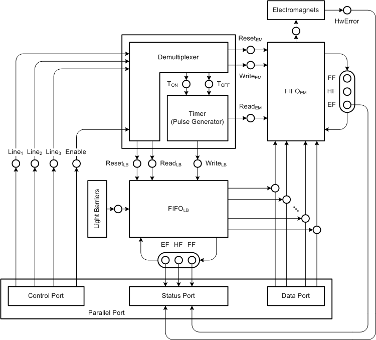
The five lines of the status port, shown in the middle of the picture, are mapped to the status register as described (bit 0 is the least-significant bit) in the following table. Please note that hardware signals may be high or low active. This means that the logic representations '0' or '1' have to be interpreted according to the respective signal. The following table also explains the coding of the status bits (special thanks to M.-P. Schapranow)
| Bit | Description | Logic '0' | Logic '1' |
|---|---|---|---|
| Bit 3 | Full flag of light barrier buffer | is not full | is full |
| Bit 4 | Empty flag of light barrier buffer | is not empty | is empty |
| Bit 5 | General hardware error flag | there is an error | there is no error |
| Bit 6 | Half full flag of light barrier buffer | is not half-full | is half-full |
| Bit 7 | Empty flag of magnet buffer | is empty | is not empty |
As an example the empty flag of the light barrier buffer can be checked like this: if((IO.ReadByte(0x0379) & 0x10) == 0).
Because of the restricted number of signals on the parallel interface, the control port is connected to a demultiplexer, which in turn provides access to the control pins of the FIFO buffers and the pulse generator (timer). In order to activate a demultiplexer output pin, it must be selected via 'Line1', 'Line2' and 'Line3'. The 'Enable' line, which is mapped to bit 0 of the control register, must be programmed at the same time. The following table shows the coding of the selection lines of the demultiplexer:
| Line1-3 | Control Register | Description |
|---|---|---|
| 0x01 | 1 = Enable demultiplexer output | |
| 0x10 | 1 = Enable interrupt on data acknowledge | |
| 0x20 | 1 = Reverse data register direction (input) | |
| 2 | 0x00 | RESET pin of both FIFO chips |
| 3 | 0x02 | Pulse generator (timer) stop |
| 4 | 0x0C | Pulse generator (timer) start |
| 5 | 0x0E | READ control pin of light barrier buffer |
| 6 | 0x08 | WRITE control pin of magnet buffer |
If the 'Enable' bit is '1', the demultiplexer is enabled and the selected pin becomes active. Please note that only one of the control pins can be active at any one time. A logic '0' of the 'Enable' bit deactivates all control pins. As an example, the RESET pin can be enabled by: IO.WriteByte(0x037A, 0x01).
Because individual signal paths differ in length, the demultiplexer output may glitch if the selected output pin is changed while the 'Enable' bit is set. The same may happen if the selected pin and state of the 'Enable' bit are changed simultaneously.
The experiment data is sampled synchronously with a frequency of 38,4 kHz into the dual-ported FIFO memory. The data can be read/written asynchronously via the parallel port by sending control signals via the control port and reading/writing the data register. Reading or writing is indicated by activating the READ or WRITE pin of the dual-ported memory chip. The technical specification of the chip can be found here. Please read the specification carefully and try to understand the functioning of the chip.
In order to control the experiment correct values must be inserted into the magnet buffer, while content of the light barrier buffer must be evaluated. During start-up the two memories must be reset as described in the chip specification. Afterwards initial values must be stored in the magnet buffer. After the start of the timer, data from the magnet buffer is transfered to the magnets, while in parallel information of the light barriers is sampled into the light barrier buffer. The control program must continously read/write new data from/to the memories. The magnet buffer must never run empty. Otherwise the experiment run will fail, while false data is send to the magnets. Depending on the number of initially provided data in the magnet buffer, the memory must be refilled slower or faster. For example an initial buffer size of 10 causes a deadline of 0,26 ms for buffer refill. The higher the initial buffer size is, the longer the deadline, but on the other hand the control delay is higher as well.
The magnets among the tube are numbered and coded as follows (the provided values must be written into the buffers) (only one magnet can be enabled at a time):
| FIFOEM Value | Description |
|---|---|
| 0x00 | No magnet enabled |
| 0x02 | Magnet 1 enabled (top of tube) |
| 0x04 | Magnet 2 enabled |
| 0x06 | Magnet 3 enabled |
| 0x08 | Magnet 4 enabled |
| 0x0a | Magnet 5 enabled |
| 0x0c | Magnet 6 enabled |
| 0x0e | Magnet 7 enabled (bottom of tube : should be enabled first) |
All other values not mentioned in this table are reserved and should not be written to the magnet FIFO.
The light barriers are positioned in the middle of two magnets with a distance of 18 cm and coded as follows:
| FIFOLB Bit | Description |
|---|---|
| Bit 0 | 1 = light barrier 1 not blocked (top of tube) |
| Bit 1 | 1 = light barrier 2 not blocked |
| Bit 2 | 1 = light barrier 3 not blocked |
| Bit 3 | 1 = light barrier 4 not blocked |
| Bit 4 | 1 = light barrier 5 not blocked |
| Bit 5 | 1 = light barrier 6 not blocked (bottom of tube) |
On the experiment-PC Windows Embedded Compact 7 is installed as operating system. You can use most the provided operating system functions and all functions from the standard C-library. The header file HIO.h is available on the experiment-PC as well. You can use all defined constants in your code by including this header-file. There is also a C frame code provided: HDLUserprogramFrame.cpp.
In this lab you have to implement a control application that shots the cylinder to the top of the tube. We provide a starting point for the implementation of the controller. In HDLUserprogramFrame.cpp you can find a frame for a control application. In the code you can find 3 procedures, nameley HDLInitialize, HDLStartClock, HDLStopClock and HDLPerform. HDLPerform provides basic I/O operations such as reading one entry from the light barrier buffer and writing one entry to the magnet buffer, keeping the number of read/written bytes synchronized. HDLStartClock and HDLStopClock start and stopp the timer, respectively. HDLInitialize resets the memories and initializes the magnet buffer with an array of entries.
- Implement the neccessary logic to reset the buffers and start/stop the timers.
- Start with a simple programm, evaluating the bits of the status register. Write a program that resets the buffers, reads the status byte, starts the timer, waits and finally reads the status byte again. Compare the changed bits of the read status byte and explain the changes.
- Implement functions for reading/writing data from/to the buffers.
- The next step is to implement an algorithm, that enables the first magnet for 900
time units. Initialize the buffers with HDL.MS7 and implement a main-loop that fills
the missing entries in the buffer, after the timer has been started. The cylinder
should jump about 25 cm. Implement the main-loop of the control algorithm by executing
HDLPerform as long as there are entries
in the light barrier buffer. Use the status register to check the empty flag of
the light barrier buffer. If the buffer is empty recheck the empty flag using sleepy
wait:
while(buffer emtpy)
Thread.Sleep(1);
// checkStatus
Make sure that there is no error condition at the other flags (e.g. empty flag of magnet buffer is on). Please write only 0 to the magnet's buffer until you are sure that the main-loop-algorithm is working. For debugging one can use the fprintf method. Remind that the usage of fprintf causes unpredictable timely behavior. Write debug output at the end of the experiment run.
Be aware that there is a watch dog running in the experiment-PC that reboots the computer if the watch dog is not signalled for 5 sec. Don't use busy wait anywhere! After a reboot you will not get any debug output. - Evaluate the bits of the read values from the light barriers. At what times does the value change if you shoot the cylinder up as described in step 5?
- Implement an algorithm that accelerates the cylinder using position information from the light barriers. Please think about the physics of the experiment first. Consider an accelerated movement including gravity.
- Have fun! And please ask if you have any problems!
Some hints for the mathematical calculations.